Our story: Development of circuit boards for small-scale production
There are many articles about setting and supporting VoIP and accessories. There are also some articles about printed circuit boards development. Other articles give hints on do-it-yourself PCBs made using laser etching. Read, for example, Laser Etching on Vynil and Homemade Arduino Mini. There are descriptions of various PCBs designing systems such as Cadence, Eagle, DipTrace or description of individual processes when developing PCBs such as information transfer from Altium to AutoCAD.
Here, I'd like to post an article about PCBs serial production based on the experience of a company and my own experience gained in other work. My task is to upgrade the existing PCB and improve the existing features and, possibly, to discover new, unprecedented horizons.
CP card coded as "G20" was taken as the basis.
Later, this board became the core for many developments of the company. It will be used with attached boards in various configurations. Several developers are engaged in the projects for these boards and each of them manages his own core and add-on PCB.
Many years ago, long before me, my company has developed a wonderful board, which, thanks to its sophisticated design, became a core for many firm's devices. The choice was made in favor of Atmel ARM9 G20, and Cyclone III by Altera was selected as a FPGA (field-programmed gate array) to connect with other boards. FPGA and CP connection is established over parallel bus compatible with the processor memory bus.
The processor operating frequency is 400MHz, two SRAM microcircuits for 512 Mbit connected over 32-bit line bus are installed on the board. In addition, fast Ethernet 10/100 and 2 host USB are installed on the board and may be used both for program downloading and for connecting Wi-Fi, network adapter and other devices. The board also contains PRI microcircuit to allow Е1/Т1 flow if connected to the telephone network.
The board is equipped with connectors for auxiliary cards. One card may be connected on the top (as a mezzanine) and two cards may be connected at the sides. Connectors are of double row type 2.54mm spaced, for through-hole soldering. The benefit is the board's affordability and availability in stores, market places and bins. The same concerns the counterparts. The disadvantages are related to its big size; due to big spacing between the contacts they have less connection lines, soldered through-hole components require much space for routing in all the board layers, and the connectors for the top card divide the board into three parts. Through-hole assembly allows for a connector orientation both upwards and downwards. Though, all the cards are usually installed over the core board.

Several submodule card types that may be structurally connected using mezzanines were developed for this board. In addition, the cards may be connected at the sides of the board using adapters.
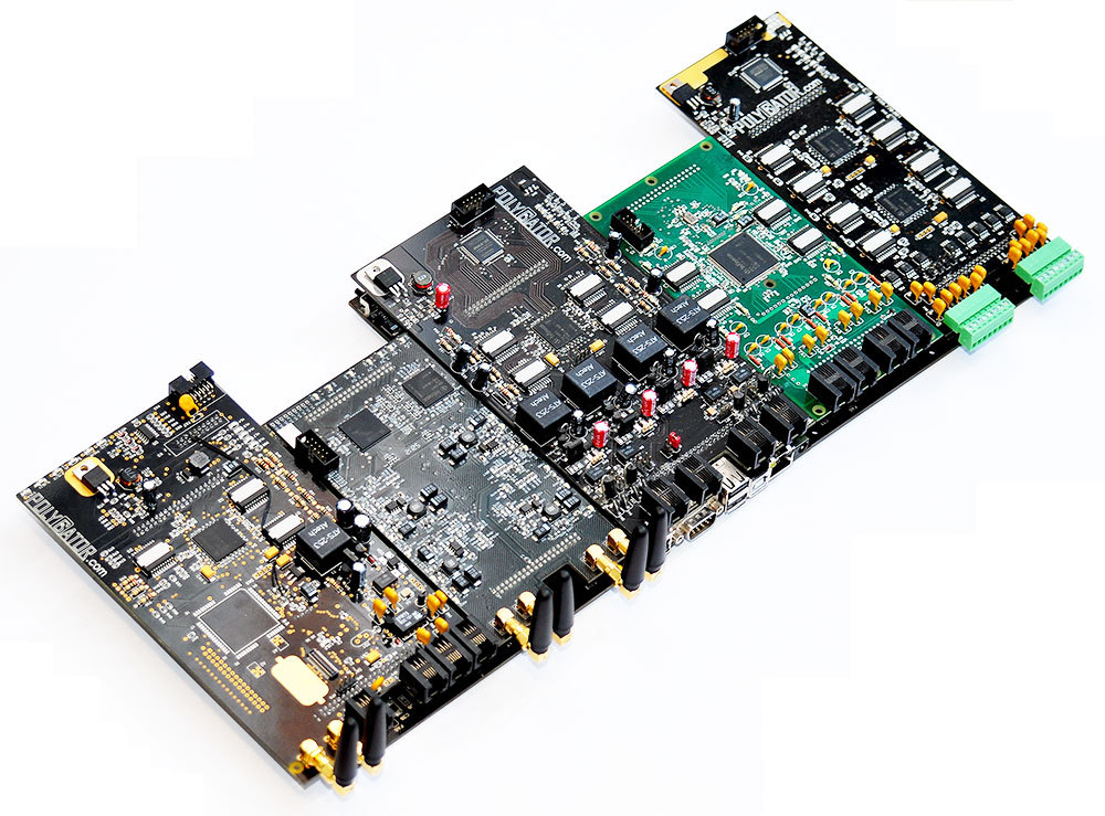
One of such modules is GSM card for four or eight channels. Removable mezzanine allowed for development of cards for various GSM modules by different firms and manufacture cards for several ranges (GSM, UMTS, WCDMA). Moreover, it allowed for installation of traditional telephony cards and for wider features PABXs. A version with SIM bank for 100 SIM cards is available.
Dividing functions between several cards allowed for individual cards setting and making upgraded mezzanine models later.
In addition, the board is used for debugging and testing individual program modules for future systems. EvBoard may be connected to its contacts to start debugging before your own PCB is made.
Then, the capabilities of the main card turned to be insufficient and it was decided to develop a new card instead of the existing one. Parallel bus restricted the data exchange speed and the number of simultaneously loaded cards. Thus, the requirements to a new board were formulated.
This board must have larger RAM, separate bus between the memory and FPGA, must be able to use fast serial channels to communicate with the cards and, preferably, must have PCIe. At the stage of components selection, additional requirements were set: built-in programmer for FPGA, two Ethernet connectors, USB-hub, HDMI, compatibility with the old PCBs. Some interfaces were included as individual connectors to connect devices in a loop.

The analysis of the available processors showed iMX6 by Freescale was the optimum. Compared to its competitors, all the documents for the processor are accessible and sane, as well as the recommendations available without a prolonged NDA signing, its BGA housing is suitable for "simple" soldering, it has an "ordinary" memory bus, floating decimal point support and a number of other advantages. It was not me who voted for ARM Cortex-A9 core, floating decimal point support and other goodies. So, we got a compromise between the possibilities of state-of-the-art mobile technologies and the production capabilities.
Circuit was derived from one of the debugging components and upgraded for our needs.

Selection of connectors for side cards is also a compromise between the desire to get multiple parallel and serial signals and the price for connectors. A pair of them may cost over USD60. The decision was made in favor of PCIe end connector. In future, this may help to reduce cost by one connector per a pair of cards. Moreover, this connector will support fast signal transmittance up to 3.125GHz as in Cyclone GX.
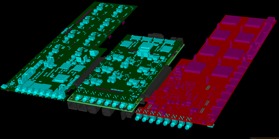
As it's not necessary to use E-Ink display, FPGA was hang to the processor parallel bus, PCIe processor bus was connected additionally together with 1Gbit FPGA bus via a high speed key. Now, our processor can send PCIe either to FPGA or to one of the side connectors. In addition to PCIe x1, four 1Gbit channels per each side are connected to the connectors. They are supposed to be used for "fast" connections in future.

3D simulation in a design package helps to avoid "closing" of critical connectors by other cards.
Then, we had to put everything into the set board size, but leave room for future field adaptation using "solder-do-not-solder" scenario. This approach allows for making a sophisticated PCB by outsourcers and adapt in for the customer's interface in house. As a result, a customer does not pay for the things he does not use. These restrictions prevent from making a compact structure sized 0201 ensuring close contact between the components. In addition, sometimes, signals need to be led outside in order to solder a bridge. This is the price of flexibility.
Therefore, other ways to save the space should be searched for.
For example, similar rating and voltage condensers may require more room by height or by area. Many microcircuits are produced in different housings and may be a significant space saving factor with similar functionality.
SOIC and QFN housings for DC-DC converters make great difference. DDPAK and TO220 housing are giants compared to them.
Texas Instruments has different types of step-down DC-DC. But modern converters can work on higher frequencies and require lesser inductivity value. With 1-2А current, 12…18uH inductivities may be found in acceptable housing sizes. If 5A current is needed, inductivity size becomes too large. Selection of another converter may help switch to 1...2uH inductivities and match the required dimensions. Both by area and height, and by weight of the components.
When designing a printed circuit board, the components interrelation should be taken into account and it is necessary to separate sensitive circuits from the sources of interference. Which, by the way, may be pulse DC-DC converters. Therefore, using shielded inductivities, compensation circuits and placing the auxiliary power sources far from the sensitive circuits may save your temper in future. When these elements cannot be separated in the PCB, various manoeuvres are required to reduce the signals effect inside the PCB.

Here, you can see the ground layer area near HF connectors inside the power layer on a GSM gateway PCI card.
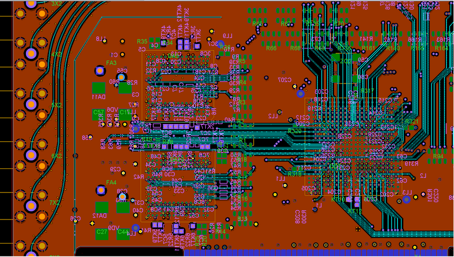
Cut out in the inner ground layer to reduce the interference between digital and HF noises on a GSM gateway PCI card.
It is worth mentioning that a PCB routing for laser etching manufacturing and factory manufacturing differs.
The requirements to the components installation also will be different.
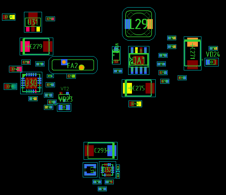
With small production batches or single prototypes production, the assemblers requirements may be like these: "I need a PCB and its components, if you have a template for SMD components installation – give it to me". Often, it is enough to have an assembly map where the components positions are marked in different color or sometime simple position designations are used. Without any accurate coordinates. Below is a piece of such assembly drawing.

If we are going to make a sophisticated PCBs or simple but big PCBs, we better deal with reputable outsource assemblers. They have the equipment for both the assembly and testing of the assembled cards. However, they have more strict requirements. Requirements to the PCB quality, template, components and even to the routing.
Process margin may be required at the PCB edges to ensure the card movement over the conveyor. This margin size depends on the manufacturer, and our manufacturers are happy with 3...5mm. If no components are installed at the card edge, process areas may be unnecessary. A card will move over the conveyor resting on its edges. For PCBs with uneven outlines, process margins may be required for smoothing the outlines to ensure the card movement over the conveyor.
Additional outfit may also be necessary to apply soldering paste. For projects with surface assembly elements, a template is usually used as such outfit. If you plan a big batch of PCBs or your PCB won't be a unique one, it's better to add library components "for production" at the early stage.
Saying "for production", I mean both assembling and the boards manufacturing.
For assemblers, it is important that all the components have right seats.
Component seat is usually slightly bigger than a soldered element to leave gaps for correction of inaccurate positioning. But, at the same time, they should not be too big. On big boards, small components may be shifted and we will have poor quality assembly. In addition, there may be too much soldering paste on a big board and, when melting, boiling flux may raise a component and put it on the side. However, with a big contact site and a smaller template hole, solder may spread over the board and won't get to the component leg.
For components with spacing between outputs less than 0.5mm, it is recommended to size an opening in the template for soldering paste smaller than the contact site to prevent from squeezing out of the soldering paste by the component and from short circuits and bridging when fusing.

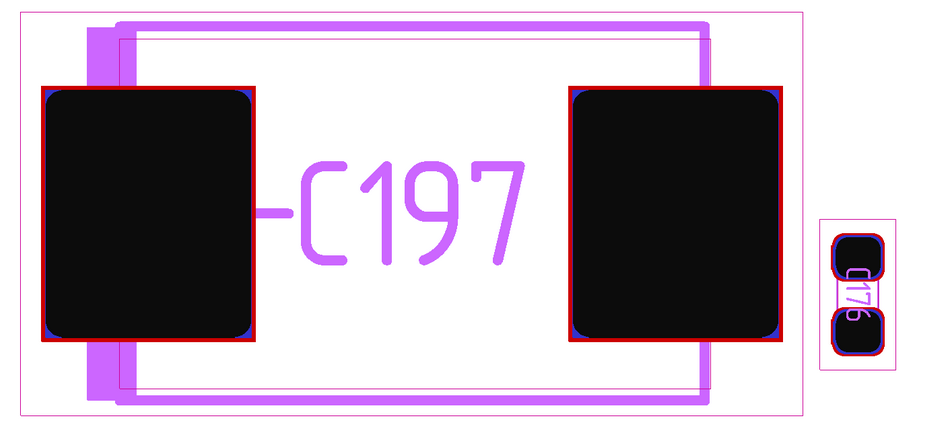
Red line on the figure shows the soldering mask opening boundary, violet line shows the contact site, and black line shows the hole in the template for soldering paste.
Today, the components are more often made in smaller sized housings and, despite high efficiency, the problem of heat removal from the microcircuits is a big challenge for the developers. So, if a housing size is small, it is impossible to remove the required quantity of heat through the cover, therefore a tricky move was invented: the microcircuit's bottom is soldered to the board and then the board takes the responsibility to remove heat over its copper layers.

I had a practical chance to test the efficiency of such cooling technique: there were microcircuits with unsoldered bottom in which thermal protection used to trip, though after soldering the bottoms, the microcircuit temperature reduced while the board temperature increased and even connectors became warm as the heat was now removed to the ground layer the connectors housing were soldered to either.
So, read the recommendation for such microcircuits seats designing thoroughly for some of them do not have another ground contact but their bottom. And if you do not put soldering paste under the contact, your microcircuit won't be electrically connected with the ground. For microcircuits with small number of legs, the thermal pad under the housing has small size, while with big microcircuits, caution is required. The manufacturers give their recommendations as for the area of the contact site and the size of the template hole for the soldering paste. Sometimes, the documents simply state 60–70% of the thermal pad area and sometimes, it is recommended to divide a big window in the template into several smaller windows to prevent from soldering paste squeezing out from big holes. The same is recommended for bit contact sites for other components such as for big inductivities.
For the component assembly system to work properly, it needs a reference point on the board and the components assembly coordinates with the turning angle. More details you can find in search results by "PCB fiducials" keyword. File with coordinates is prepared in PCB designing software automatically.
In the end, I usually have a file like below with tabulations:
Header:
$HEADER$
BOARD_TYPE PCB_DESIGN
UNITS MM
$END HEADER
Part with components:
$PART_SECTION_BEGIN$
R303 RC0402FR-0768KL 270.00 120.30 39.10 BOTTOM YES
C580 CC0402-KR-X5R-5BB-104 180.00 38.40 88.50 BOTTOM YES
VT3 NDS331N 90.00 56.80 26.40 TOP NO
…
C282 CC0402-KR-X5R-7BB-104 180.00 128.10 26.20 BOTTOM YES
VS2 BZT52C-3V3 90.00 71.40 27.10 BOTTOM YES
U23 MCIMX6Q4AVT08AC 0.00 106.00 45.90 TOP NO
$PART_SECTION_END$
Coordinates with fiducials:
$FIDUCIAL_SECTION_BEGIN$
BOARD 42.50 8.00 BOTTOM
BOARD 177.00 8.00 BOTTOM
BOARD 183.40 113.50 BOTTOM
BOARD 183.40 113.50 TOP
BOARD 177.00 8.00 TOP
BOARD 42.50 8.00 TOP
U23 94.50 57.40 TOP
U23 117.50 34.40 TOP
U10 22.70 87.00 TOP
U10 38.70 109.00 TOP
U18 52.50 69.50 TOP
U18 81.50 98.50 TOP
$FIDUCIAL_SECTION_END$
For small sized PCBs, a group blank or a panel is the beast layout option. This requirement is set by both PCB pad manufacturers and the assemblers. For assembly, coordinates of components for one PCB, cards spacing in the blank and the card angle in the blank are provided.
PCBs require rotating mostly for reducing the bank area in case of an uneven PCB outline. At the same time, rectangular boards also may be rotated in the panel. Once, our assemblers demanded increasing the process margin from 5mm to 30mm for one of the board sides as there were components to be installed with a very small spacing. After grouping the boards into a panel, the problem edge was turned inside and the process margin was kept 5mm everywhere. This allowed for placing two panels in one big glass fiber sheet at the production stage. And the customer was able to keep his costs at the level.

Gas flow meter boards manufacturing panel.
After assembling, the boards may be separated either by the assembler, or easily by us. Then goes testing, firmware installation, setting, housing and pre-sale preparation.
These are just several stages of the boards and devices preparation for production. They may be supplemented by components list minimizing, manufacturability testing, housing design and components positioning on the board together with other operations, but I tried to describe the operations I used to do personally.
P.S. I do not have a photo of a new board, as it's not delivered yet. Currently, a new board is developed in the old board size based on the new layout and without unnecessary fancy things such as a display, expensive FPGA, etc.
Contact Details
POLYGATOR (manufacturer)
This email address is being protected from spambots. You need JavaScript enabled to view it.
www.polygator.com
Skype: polygator
Contacts:
UKRAINE:
+380(56)719-9030 (Office Landline)
+380(67)527-4171 (Mob/Telegram)
UK: +44(203)769-1858 (Virt.Landline)
USA: +1(312)940-6939 (Virt.Landline)
Compatibility Short-list
| Native drivers | Certified with | Tested with | Technologies |
| Asterisk (PCI GSM Interface Card for 4/8 SIM-cards) |
SoftSwitch, IP-PBX |
GSM UMTS PRI(E1) SMS |
Website by wwsiter